位置:CDCU877ZQL > CDCU877ZQL详情
CDCU877ZQL中文资料
CDCU877ZQL数据手册规格书PDF详情
FEATURES
· 1.8-V Phase Lock Loop Clock Driver for
Double Data Rate (DDR II) Applications
· Spread Spectrum Clock Compatible
· Operating Frequency: 10 MHz to 400 MHz
· Low Current Consumption: <135 mA
· Low Jitter (Cycle-Cycle): ±30 ps
· Low Output Skew: 35 ps
· Low Period Jitter: ±20 ps
· Low Dynamic Phase Offset: ±15 ps
· Low Static Phase Offset: ±50 ps
· Distributes One Differential Clock Input to Ten
Differential Outputs
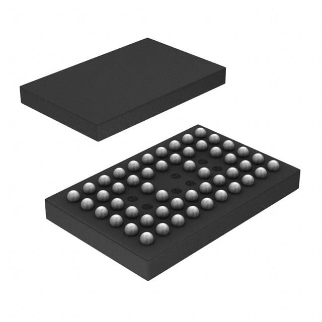
· 52-Ball μBGA (MicroStar™ Junior BGA,
0,65-mm pitch) and 40-Pin MLF
· External Feedback Pins (FBIN, FBIN) are Used
to Synchronize the Outputs to the Input
Clocks
· Meets or Exceeds JESD82-8 PLL Standard for
PC2-3200/4300
· Fail-Safe Inputs
DESCRIPTION
The CDCU877 is a high-performance, low-jitter, low-skew, zero-delay buffer that distributes a differential clock
input pair (CK, CK) to ten differential pairs of clock outputs (Yn, Yn) and to one differential pair of feedback clock
outputs (FBOUT, FBOUT). The clock outputs are controlled by the input clocks (CK, CK), the feedback clocks
(FBIN, FBIN), the LVCMOS control pins (OE, OS), and the analog power input (AVDD). When OE is low, the
clock outputs, except FBOUT/FBOUT, are disabled while the internal PLL continues to maintain its locked-in
frequency. OS (output select) is a program pin that must be tied to GND or VDD. When OS is high, OE functions
as previously described. When OS and OE are both low, OE has no affect on Y7/Y7, they are free running.
When AVDD is grounded, the PLL is turned off and bypassed for test purposes.
When both clock inputs (CK, CK) are logic low, the device enters in a low power mode. An input logic detection
circuit on the differential inputs, independent from input buffers, detects the logic low level and performs in a low
power state where all outputs, the feedback, and the PLL are off. When the clock inputs transition from being
logic low to being differential signals, the PLL turns back on, the inputs and the outputs are enabled, and the
PLL obtains phase lock between the feedback clock pair (FBIN, FBIN) and the clock input pair (CK, CK) within
the specified stabilization time.
The CDCU877 is able to track spread spectrum clocking (SSC) for reduced EMI. This device operates from
—40°C to 85°C.
CDCU877ZQL产品属性
- 类型
描述
- 型号
CDCU877ZQL
- 功能描述
时钟驱动器及分配 1.8v PLL Clock Driver
- RoHS
否
- 制造商
Micrel
- 1
4
- 输出类型
Differential
- 最大输出频率
4.2 GHz
- 电源电压-最小
5 V
- 最大工作温度
+ 85 C
- 封装/箱体
SOIC-8
- 封装
Reel
| 供应商 | 型号 | 品牌 | 批号 | 封装 | 库存 | 备注 | 价格 |
|---|---|---|---|---|---|---|---|
TI |
24+ |
BGA |
7850 |
只做原装正品现货或订货假一赔十! |
|||
TI/德州仪器 |
21+ |
BGA |
23000 |
只做正品原装现货 |
|||
TI |
23+ |
BGA |
50000 |
全新原装正品现货,支持订货 |
|||
TI |
25+ |
BGA |
8880 |
原装认准芯泽盛世! |
|||
TI |
12+ |
BGA |
25 |
一级代理,专注军工、汽车、医疗、工业、新能源、电力 |
|||
TI/德州仪器 |
24+ |
BGA |
1500 |
只供应原装正品 欢迎询价 |
|||
22+ |
5000 |
||||||
TI |
23+ |
BGA |
5000 |
全新原装,支持实单,非诚勿扰 |
|||
TI |
23+ |
BGA |
2525 |
原厂原装正品 |
|||
TI |
23+ |
BGA |
3200 |
公司只做原装,可来电咨询 |
CDCU877ZQLT 价格
参考价格:¥44.1505
CDCU877ZQL 资料下载更多...
CDCU877ZQL 芯片相关型号
- 3336
- 58531-3
- 58536-1
- 7-1579005-1
- 981HE3B4WCPXXXXBO10E1
- 981HE3B4WCSXXXXBO10E1
- 981HE3B4WCZXXXXBO10E1
- A12108CH
- A12108CHNF
- A1210CH
- A1210CHNF
- A1210CHNFS
- A1210CHS
- CE8
- CQ1608X7R474M100ALB
- CQ1608X7R474M100ARB
- CQ1608X7R474M160ALB
- CQ1608X7R474M160ARB
- CQ1608X7R474M250ALB
- CQ1608X7R474M250ARB
- CQ1608X7R474M350ALB
- CQ1608X7R474M350ARB
- CQ1608X7R474M500ALB
- CQ1608X7R474M500ARB
- CQ1608X7R474M6R3ALB
- CQ1608X7R474M6R3ARB
- LDC1614
- MUR1520
Datasheet数据表PDF页码索引
- P1
- P2
- P3
- P4
- P5
- P6
- P7
- P8
- P9
- P10
- P11
- P12
- P13
- P14
- P15
- P16
- P17
- P18
- P19
- P20
- P21
- P22
- P23
- P24
- P25
- P26
- P27
- P28
- P29
- P30
- P31
- P32
- P33
- P34
- P35
- P36
- P37
- P38
- P39
- P40
- P41
- P42
- P43
- P44
- P45
- P46
- P47
- P48
- P49
- P50
- P51
- P52
- P53
- P54
- P55
- P56
- P57
- P58
- P59
- P60
- P61
- P62
- P63
- P64
- P65
- P66
- P67
- P68
- P69
- P70
- P71
- P72
- P73
- P74
- P75
- P76
- P77
- P78
- P79
- P80
- P81
- P82
- P83
- P84
- P85
- P86
- P87
- P88
- P89
- P90
- P91
- P92
- P93
- P94
- P95
- P96
- P97
- P98
- P99
- P100
- P101
- P102
- P103
- P104
- P105
