位置:CDCU877RTB > CDCU877RTB详情
CDCU877RTB中文资料
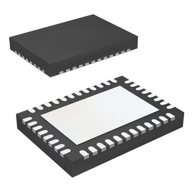
CDCU877RTB数据手册规格书PDF详情
FEATURES
· 1.8-V Phase Lock Loop Clock Driver for
Double Data Rate (DDR II) Applications
· Spread Spectrum Clock Compatible
· Operating Frequency: 10 MHz to 400 MHz
· Low Current Consumption: <135 mA
· Low Jitter (Cycle-Cycle): ±30 ps
· Low Output Skew: 35 ps
· Low Period Jitter: ±20 ps
· Low Dynamic Phase Offset: ±15 ps
· Low Static Phase Offset: ±50 ps
· Distributes One Differential Clock Input to Ten
Differential Outputs
· 52-Ball μBGA (MicroStar™ Junior BGA,
0,65-mm pitch) and 40-Pin MLF
· External Feedback Pins (FBIN, FBIN) are Used
to Synchronize the Outputs to the Input
Clocks
· Meets or Exceeds JESD82-8 PLL Standard for
PC2-3200/4300
· Fail-Safe Inputs
DESCRIPTION
The CDCU877 is a high-performance, low-jitter, low-skew, zero-delay buffer that distributes a differential clock
input pair (CK, CK) to ten differential pairs of clock outputs (Yn, Yn) and to one differential pair of feedback clock
outputs (FBOUT, FBOUT). The clock outputs are controlled by the input clocks (CK, CK), the feedback clocks
(FBIN, FBIN), the LVCMOS control pins (OE, OS), and the analog power input (AVDD). When OE is low, the
clock outputs, except FBOUT/FBOUT, are disabled while the internal PLL continues to maintain its locked-in
frequency. OS (output select) is a program pin that must be tied to GND or VDD. When OS is high, OE functions
as previously described. When OS and OE are both low, OE has no affect on Y7/Y7, they are free running.
When AVDD is grounded, the PLL is turned off and bypassed for test purposes.
When both clock inputs (CK, CK) are logic low, the device enters in a low power mode. An input logic detection
circuit on the differential inputs, independent from input buffers, detects the logic low level and performs in a low
power state where all outputs, the feedback, and the PLL are off. When the clock inputs transition from being
logic low to being differential signals, the PLL turns back on, the inputs and the outputs are enabled, and the
PLL obtains phase lock between the feedback clock pair (FBIN, FBIN) and the clock input pair (CK, CK) within
the specified stabilization time.
The CDCU877 is able to track spread spectrum clocking (SSC) for reduced EMI. This device operates from
—40°C to 85°C.
CDCU877RTB产品属性
- 类型
描述
- 型号
CDCU877RTB
- 制造商
TI
- 制造商全称
Texas Instruments
- 功能描述
1.8-V PHASE LOCK LOOP CLOCK DRIVER
| 供应商 | 型号 | 品牌 | 批号 | 封装 | 库存 | 备注 | 价格 |
|---|---|---|---|---|---|---|---|
24+ |
SOP16 |
6000 |
美国德州仪器TEXASINSTRUMENTS原厂代理辉华拓展内地现 |
||||
TI(德州仪器) |
24+ |
QFN40EP(6x6) |
2669 |
只做原装,提供一站式配单服务,代工代料。BOM配单 |
|||
TI/德州仪器 |
25+ |
原厂封装 |
10000 |
||||
TI |
24+ |
7500 |
40-QFN |
||||
TI |
2015+ |
SOP |
19889 |
一级代理原装现货,特价热卖! |
|||
TI |
16+ |
40-QFN |
2500 |
全新进口原装 |
|||
TI |
16+ |
VQFN |
10000 |
原装正品 |
|||
TI |
20+ |
QFN |
53650 |
TI原装主营-可开原型号增税票 |
|||
Texas Instruments |
24+ |
40-VQFN-EP(6x6) |
53200 |
一级代理/放心采购 |
|||
TI/德州仪器 |
23+ |
40-QFN |
2500 |
原装正品代理渠道价格优势 |
CDCU877RTBT 价格
参考价格:¥38.9724
CDCU877RTB 资料下载更多...
CDCU877RTB 芯片相关型号
- 0402S104C
- 0402S104D
- 0402S104J
- 0402S104M
- 451279SSH04TXND
- 451279SSH04TXNH
- 451279SSH04TXNZ
- 451279SSH04TXSG
- AC1210DR-10
- CD74ACT00M
- CD74ACT00M96
- CD74ACT00M96.A
- CD74ACT00M96G4.A
- CDCU877ARTB
- CDCU877AZQL
- CDCU877GQL
- CDCU877RHA
- GS40T20
- PCSB350-10S-2Y
- PCSB350-12S-1Y
- PCSB350-14S-1Y
- PCSB350-2S-4Y
- PCSB350-3S-4Y
- PCSB350-4S-3Y
- PCSB350-5S-3Y
- PCSB350-6S-2Y
- V62SLASH24606-01XE
- V62SLASH24611-01XE
Datasheet数据表PDF页码索引
- P1
- P2
- P3
- P4
- P5
- P6
- P7
- P8
- P9
- P10
- P11
- P12
- P13
- P14
- P15
- P16
- P17
- P18
- P19
- P20
- P21
- P22
- P23
- P24
- P25
- P26
- P27
- P28
- P29
- P30
- P31
- P32
- P33
- P34
- P35
- P36
- P37
- P38
- P39
- P40
- P41
- P42
- P43
- P44
- P45
- P46
- P47
- P48
- P49
- P50
- P51
- P52
- P53
- P54
- P55
- P56
- P57
- P58
- P59
- P60
- P61
- P62
- P63
- P64
- P65
- P66
- P67
- P68
- P69
- P70
- P71
- P72
- P73
- P74
- P75
- P76
- P77
- P78
- P79
- P80
- P81
- P82
- P83
- P84
- P85
- P86
- P87
- P88
- P89
- P90
- P91
- P92
- P93
- P94
- P95
- P96
- P97
- P98
- P99
- P100
- P101
- P102
- P103
- P104
- P105