位置:CY7C1618KV18-333BZXC > CY7C1618KV18-333BZXC详情
CY7C1618KV18-333BZXC中文资料
CY7C1618KV18-333BZXC数据手册规格书PDF详情
Functional Description
The CY7C1618KV18, and CY7C1620KV18 are 1.8-V synchronous pipelined SRAM equipped with DDR II architecture. The DDR II consists of an SRAM core with advanced synchronous peripheral circuitry and a 1-bit burst counter. Addresses for read and write are latched on alternate rising edges of the input (K) clock. Write data is registered on the rising edges of both K and K. Read data is driven on the rising edges of C and C if provided, or on the rising edge of K and K if C/C are not provided. On CY7C1618KV18 and CY7C1620KV18, the burst counter takes in the least significant bit of the external address and bursts two 18-bit words in the case of CY7C1618KV18 and two 36-bit words in the case of CY7C1620KV18 sequentially into or out of the device.
Features
■ 144-Mbit density (8M × 18, 4M × 36)
■ 333 MHz clock for high bandwidth
■ Two-word burst for reducing address bus frequency
■ Double data rate (DDR) interfaces (data transferred at 666 MHz) at 333 MHz
■ Two input clocks (K and K) for precise DDR timing
❐ SRAM uses rising edges only
■ Two input clocks for output data (C and C) to minimize clock skew and flight time mismatches
■ Echo clocks (CQ and CQ) simplify data capture in high-speed systems
■ Synchronous internally self-timed writes
■ DDR II operates with 1.5-cycle read latency when DOFF is asserted high
■ Operates similar to DDR I device with one cycle read latency when DOFF is asserted low
■ 1.8-V core power supply with high-speed transceiver logic (HSTL) inputs and outputs
■ Variable drive HSTL output buffers
■ Expanded HSTL output voltage (1.4 V–VDD)
❐ Supports both 1.5-V and 1.8-V I/O supply
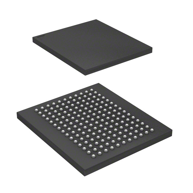
■ Available in 165-ball fine-pitch ball grid array (FBGA) package (15 × 17 × 1.4 mm)
■ Offered in Pb-free packages
■ JTAG 1149.1 compatible test access port
■ Phase locked loop (PLL) for accurate data placement
| 供应商 | 型号 | 品牌 | 批号 | 封装 | 库存 | 备注 | 价格 |
|---|---|---|---|---|---|---|---|
Cypress |
165-FBGA |
7510 |
Cypress一级分销,原装原盒原包装! |
||||
CYPRESS |
25+ |
BGA-165 |
105 |
就找我吧!--邀您体验愉快问购元件! |
|||
Cypress |
25+ |
电联咨询 |
7800 |
公司现货,提供拆样技术支持 |
|||
Cypress Semiconductor Corp |
25+ |
165-LBGA |
9350 |
独立分销商 公司只做原装 诚心经营 免费试样正品保证 |
|||
Cypress Semiconductor/赛普拉斯 |
两年内 |
NA |
308 |
实单价格可谈 |
|||
CYPRESS/赛普拉斯 |
24+ |
FBGA-165 |
39900 |
只做原装进口现货 |
|||
CYPRESS/赛普拉斯 |
20+ |
FBGA-165 |
1050 |
||||
CYPRESS(赛普拉斯) |
24+ |
LBGA165 |
7350 |
现货供应,当天可交货!免费送样,原厂技术支持!!! |
|||
Cypress Semiconductor Corp |
23+ |
165-FBGA15x17 |
7300 |
专注配单,只做原装进口现货 |
|||
CYPRESS/赛普拉斯 |
20+ |
FBGA-165 |
1 |
进口原装现货假一赔万力挺实单 |
CY7C1618KV18-333BZXC 资料下载更多...
CY7C1618KV18-333BZXC 芯片相关型号
- 030608-1
- 1700021072-01
- 1701200220
- 1750000400
- 2070013483
- 310-91-147-41-001000
- 9666226300E
- 96PSA-A60W12P2-1
- CY7C1556KV18
- CY7C1663KV18
- ITA-EM-ST61-10A1E
- KBLA-1
- LDG5AP-4M4N-35-1
- MIC-7500B-S9A1E
- MIOe-230
- NCS3-72+
- PCE-5B05-02A1E
- UC3842AD8G4
- UCC1806-SP
- UCC2580DTR-1G4
- UCC2806DG4
- UCC2808APW-1
- UCC28221D
- UCC28521DWR
- UCC3580DTR-4
- UCC3806PWTR
- ULV4F2BSSG353
- ULV7F2G1SG606
- ULV7F2HSSG6Q5
- ULV8F2GS1G3Q7
CYPRESS相关芯片制造商
Datasheet数据表PDF页码索引
- P1
- P2
- P3
- P4
- P5
- P6
- P7
- P8
- P9
- P10
- P11
- P12
- P13
- P14
- P15
- P16
- P17
- P18
- P19
- P20
- P21
- P22
- P23
- P24
- P25
- P26
- P27
- P28
- P29
- P30
- P31
- P32
- P33
- P34
- P35
- P36
- P37
- P38
- P39
- P40
- P41
- P42
- P43
- P44
- P45
- P46
- P47
- P48
- P49
- P50
- P51
- P52
- P53
- P54
- P55
- P56
- P57
- P58
- P59
- P60
- P61
- P62
- P63
- P64
- P65
- P66
- P67
- P68
- P69
- P70
- P71
- P72
- P73
- P74
- P75
- P76
- P77
- P78
- P79
- P80
- P81
- P82
- P83
- P84
- P85
- P86
- P87
- P88
- P89
- P90
- P91
- P92
- P93
- P94
- P95
- P96
- P97
- P98
- P99
- P100
- P101
- P102
- P103
- P104
- P105
- P106
- P107