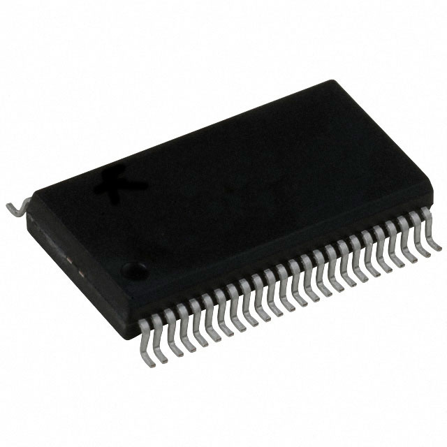
位置:SN75LVDS84ADGGR > SN75LVDS84ADGGR详情
SN75LVDS84ADGGR中文资料
SN75LVDS84ADGGR数据手册规格书PDF详情
21:3 Data Channel Compression at up to
196 Million Bytes per Second Throughput
Suited for SVGA, XGA, or SXGA Data
Transmission From Controller to Display
With Very Low EMI
21 Data Channels Plus Clock In
Low-Voltage TTL Inputs and 3 Data
Channels Plus Clock Out Low-Voltage
Differential Signaling (LVDS) Outputs
Operates From a Single 3.3-V Supply and
89 mW (Typ)
Ultralow-Power 3.3-V CMOS Version of the
SN75LVDS84. Power Consumption About
One Third of the ’LVDS84
Packaged in Thin Shrink Small-Outline
Package (TSSOP) With 20 Mil Terminal
Pitch
Consumes Less Than 0.54 mW When
Disabled
Wide Phase-Lock Input Frequency Range:
31 MHz to 75 MHz
No External Components Required for PLL
Outputs Meet or Exceed the Requirements
of ANSI EIA/TIA-644 Standard
SSC Tracking Capability of 3% Center
Spread at 50-kHz Modulation Frequency
Improved Replacement for SN75LVDS84
and NSC’s DS90CF363A 3-V Device
Available in Q-Temp Automotive
High Reliability Automotive Applications
Configuration Control / Print Support
Qualification to Automotive Standards
description
The SN75LVDS84A and SN65LVDS84AQ FlatLink transmitters contains three 7-bit parallel-load serial-out shift
registers, and four low-voltage differential signaling (LVDS) line drivers in a single integrated circuit. These
functions allow 21 bits of single-ended LVTTL data to be synchronously transmitted over 3 balanced-pair
conductors for receipt by a compatible receiver, such as the SN75LVDS82 or SN75LVDS86/86A.
When transmitting, data bits D0 – D20 are each loaded into registers of the ’LVDS84A upon the falling edge.
The internal PLL is frequency-locked to CLKIN and then used to unload the data registers in 7-bit slices. The
three serial streams and a phase-locked clock (CLKOUT) are then output to LVDS output drivers. The frequency
of CLKOUT is the same as the input clock, CLKIN.
The ’LVDS84A requires no external components and little or no control. The data bus appears the same at the
input to the transmitter and output of the receiver with the data transmission transparent to the user(s). The only
user intervention is the possible use of the shutdown/clear (SHTDN) active-low input to inhibit the clock and shut
off the LVDS output drivers for lower power consumption. A low-level on this signal clears all internal registers
to a low level.
The SN75LVDS84A is characterized for operation over ambient free-air temperatures of 0°C to 70°C. The
SN65LVDS84AQ is characterized for operation over the full Automotive temperature range of –40°C to 125°C.
SN75LVDS84ADGGR产品属性
- 类型
描述
- 型号
SN75LVDS84ADGGR
- 功能描述
总线发射器 Flatlink
- RoHS
否
- 制造商
Texas Instruments
- 数据速率
135 Mpps
- 电源电压-最大
3.6 V
- 电源电压-最小
3 V
- 最大工作温度
+ 70 C
- 安装风格
SMD/SMT
- 封装/箱体
TSSOP-56
- 封装
Reel
| 供应商 | 型号 | 品牌 | 批号 | 封装 | 库存 | 备注 | 价格 |
|---|---|---|---|---|---|---|---|
TI/德州仪器 |
25+ |
TSSOP48 |
12496 |
TI/德州仪器原装正品SN75LVDS84ADGGR即刻询购立享优惠#长期有货 |
|||
TEXASINSTRUMENTS |
2012 |
TSSOP-48 |
4000 |
进口原装现货,假一赔十 |
|||
TI |
20+ |
TSSOP48 |
6000 |
原装正品公司现货假一赔十 |
|||
主营TI |
2021+ |
TSSOP |
9450 |
原装现货。 |
|||
TI |
23+ |
TSSOP-48 |
30000 |
全新原装正品 |
|||
TI/德州仪器 |
22+ |
TSSOP-48 |
500000 |
原装现货支持实单价优/含税 |
|||
TI/德州仪器 |
2021+ |
TSSOP48 |
9000 |
原装现货,随时欢迎询价 |
|||
TI/德州仪器 |
2023+ |
SMD |
53200 |
正品,原装现货 |
|||
TI(德州仪器) |
24+ |
TSSOP-48-6 |
9203 |
支持大陆交货,美金交易。原装现货库存。 |
|||
TI/德州仪器 |
25+ |
TSSOP-48 |
4987 |
强势库存!绝对原装公司现货! |
SN75LVDS84ADGGR 价格
参考价格:¥15.2079
SN75LVDS84ADGGR 资料下载更多...
SN75LVDS84ADGGR 芯片相关型号
- 1658-G41-08-S80-10A
- 1658-G41-08-S80-12A
- 1658-G41-08-S80-15A
- 1658-G41-08-S80-20A
- 1658-G41-08-S80-25A
- 1658-G41-08-S80-5A
- 22J50KE
- ECQE2395KBB
- ECQE2395KBD
- ECS-200-10-33Q-CWM-TR3
- ECS-200-10-33Q-CWN-TR
- ECS-200-10-33Q-CWN-TR3
- ECS-200-10-33Q-CWP-TR
- ECS-200-10-33Q-CWP-TR3
- ECS-200-10-33Q-CWS-TR
- ECS-200-10-33Q-CWS-TR3
- ECS-200-10-33Q-CWU-TR
- ECS-200-10-33Q-CWU-TR3
- ECS-200-10-33Q-CWY-TR3
- PX2AG1XX1.6B
- SN74V293-EP
- SN75LVDS84ADGG.A
- SN75LVDS84ADGGR.A
- SN75LVDS84ADGGRG4.A
- SN75LVDS86A
- SN75LVDS86ADGG
- SN75LVDS86ADGG.A
- SN75LVDS86ADGGR
- SN75LVDS86ADGGR.A
- SN75LVDS86ADGGRG4.A
Datasheet数据表PDF页码索引
- P1
- P2
- P3
- P4
- P5
- P6
- P7
- P8
- P9
- P10
- P11
- P12
- P13
- P14
- P15
- P16
- P17
- P18
- P19
- P20
- P21
- P22
- P23
- P24
- P25
- P26
- P27
- P28
- P29
- P30
- P31
- P32
- P33
- P34
- P35
- P36
- P37
- P38
- P39
- P40
- P41
- P42
- P43
- P44
- P45
- P46
- P47
- P48
- P49
- P50
- P51
- P52
- P53
- P54
- P55
- P56
- P57
- P58
- P59
- P60
- P61
- P62
- P63
- P64
- P65
- P66
- P67
- P68
- P69
- P70
- P71
- P72
- P73
- P74
- P75
- P76
- P77
- P78
- P79
- P80
- P81
- P82
- P83
- P84
- P85
- P86
- P87
- P88
- P89
- P90
- P91
- P92
- P93
- P94
- P95
- P96
- P97
- P98
- P99
- P100
- P101
- P102
- P103
- P104
- P105
