位置:TDA4VM > TDA4VM详情
TDA4VM中文资料
TDA4VM数据手册规格书PDF详情
1 Features
Processor cores:
• C7x floating point, vector DSP, up to 1.0GHz, 80
GFLOPS, 256 GOPS
• Deep-learning matrix multiply accelerator (MMA),
up to 8 TOPS (8b) at 1.0GHz
• Vision Processing Accelerators (VPAC) with Image
Signal Processor (ISP) and multiple vision assist
accelerators
• Depth and Motion Processing Accelerators
(DMPAC)
• Dual 64-bit Arm® Cortex®-A72 microprocessor
subsystem at up to 2.0GHz
– 1MB shared L2 cache per dual-core Cortex®-
A72 cluster
– 32KB L1 DCache and 48KB L1 ICache per
Cortex®-A72 core
• Six Arm® Cortex®-R5F MCUs at up to 1.0GHz
– 16K I-Cache, 16K D-Cache, 64K L2 TCM
– Two Arm® Cortex®-R5F MCUs in isolated MCU
subsystem
– Four Arm® Cortex®-R5F MCUs in general
compute partition
• Two C66x floating point DSP, up to 1.35GHz,
40GFLOPS, 160GOPS
• 3D GPU PowerVR® Rogue 8XE GE8430, up to
750MHz, 96GFLOPS, 6Gpix/sec
• Custom-designed interconnect fabric supporting
near max processing entitlement
Memory subsystem:
• Up to 8MB of on-chip L3 RAM with ECC and
coherency
– ECC error protection
– Shared coherent cache
– Supports internal DMA engine
• External Memory Interface (EMIF) module with
ECC
– Supports LPDDR4 memory types
– Supports speeds up to 4266MT/s
– 32-bit data bus with inline ECC
• General-Purpose Memory Controller (GPMC)
• 512KB on-chip SRAM in MAIN domain, protected
by ECC
Functional Safety:
• Functional Safety-Compliant targeted (on select
part numbers)
– Developed for functional safety applications
– Documentation will be available to aid ISO
26262/IEC 61508 functional safety system
design up to ASIL-D/SIL-3 targeted
– Systematic capability up to ASIL-D/SC-3
targeted
– Hardware integrity up to ASIL-D/SIL-3 targeted
for MCU Domain
– Hardware integrity up to ASIL-B/SIL-2 targeted
for Main Domain
– Safety-related certifications
• ISO 26262 certification up to ASIL-D by TÜV
SÜD planned
• IEC 61508 certification up to SIL-3 by TÜV
SÜD planned
• AEC-Q100 qualified on part number variants
ending in Q1
Device security (on select part numbers):
• Secure boot with secure run-time support
• Customer programmable root key, up to RSA-4K
or ECC-512
• Embedded hardware security module
• Crypto hardware accelerators – PKA with ECC,
AES, SHA, RNG, DES and 3DES
High speed serial interfaces:
• Integrated Ethernet switch supporting up to 8
external ports
– All ports support 2.5Gb SGMII
– All ports support 1Gb SGMII/RGMII
– All ports support 100Mb RMII
– Any two ports support QSGMII (using 4 internal
ports per QSGMII)
• Up to four PCI-Express® (PCIe) Gen3 controllers
– Up to two lanes per controller
– Gen1 (2.5GT/s), Gen2 (5.0GT/s), and Gen3
(8.0GT/s) operation with auto-negotiation
• Two USB 3.0 dual-role device (DRD) subsystem
– Two enhanced SuperSpeed Gen1 Ports
– Each port supports Type-C switching
– Each port independently configurable as USB
host, USB peripheral, or USB DRD
Automotive interfaces:
• Sixteen Modular Controller Area Network (MCAN)
modules with full CAN-FD support
• Two CSI2.0 4L RX plus One CSI2.0 4L TX
– 2.5Gbps RX throughput per lane (20Gbps total)
• DOinsep leaDyP s/uDbPs iynsteterfmac:e with Multi-Display Support
(MST)
– HDCP1.4/HDCP2.2 high-bandwidth digital
content protection
• One DSI TX (up to 2.5K)
• Up to two DPI
Audio interfaces:
• Twelve Multichannel Audio Serial Port (MCASP)
modules
Video acceleration:
• Ultra-HD video, one (3840 × 2160p, 60 fps), or two
(3840 × 2160p, 30 fps) H.264/H.265 decode
• Full-HD video, four (1920 × 1080p, 60 fps), or eight
(1920 × 1080p, 30 fps) H.264/H.265 decode
• Full-HD video, one (1920 × 1080p, 60 fps), or up to
three (1920 × 1080p, 30 fps) H.264 encode
Flash memory interfaces:
• Embedded MultiMediaCard Interface ( eMMC™
5.1)
• Universal Flash Storage (UFS 2.1) interface with
two lanes
• Two Secure Digital® 3.0/Secure Digital Input
Output 3.0 interfaces (SD3.0/SDIO3.0)
• Two simultaneous flash interfaces configured as
– One OSPI and one QSPI flash interfaces
– or one HyperBus™ and one QSPI flash
interface
System-on-Chip (SoC) architecture:
• 16-nm FinFET technology
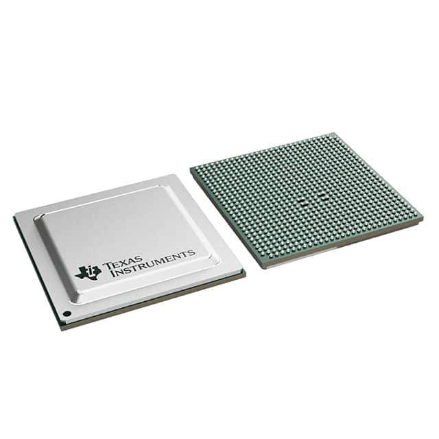
• 24 mm × 24 mm, 0.8-mm pitch, 827-pin FCBGA
(ALF), enables IPC class 3 PCB routing
TPS6594-Q1 Companion Power Management
ICs (PMIC):
• Functional Safety support up to ASIL-D
• Flexible mapping to support different use cases
2 Applications
• Advanced surround view and park assistance systems
• Autonomous sensor fusion / perception systems including camera, radar and lidar sensors
• Mono and multi-sensor Front camera systems
• Next generation eMirror systems
• Industrial mobile robot (AGV/AMR) with safety functions
• Machine vision
• Smart retail
• Smart shopping cart
• Construction and agriculture
• Edge AI BOX
• Single Board Computer
• Off-highway vehicle control
• Industrial PC with AI
3 Description
The TDA4VM processor family targeted at ADAS and Autonomous Vehicle (AV) applications and built on
extensive market knowledge accumulated over a decade of TI’s leadership in the ADAS processor market.
The unique combination high-performance compute, deep-learning engine, dedicated accelerators for signal
and image processing in a functional safety compliant targeted architecture make the TDA4VM devices a
great fit for several industrial applications, such as: Robotics, Machine Vision, Radar, and so on. The TDA4VM
provides high performance compute for both traditional and deep learning algorithms at industry leading power/
performance ratios with a high level of system integration to enable scalability and lower costs for advanced
automotive platforms supporting multiple sensor modalities in centralized ECUs or stand-alone sensors. Key
cores include next generation DSP with scalar and vector cores, dedicated deep learning and traditional
algorithm accelerators, latest Arm and GPU processors for general compute, an integrated next generation
imaging subsystem (ISP), video codec, Ethernet hub and isolated MCU island. All protected by automotive grade
safety and security hardware accelerators.
Key Performance Cores Overview
The “C7x” next generation DSP combines TI’s industry leading DSP and EVE cores into a single higher
performance core and adds floating point vector calculation capabilities, enabling backward compatibility for
legacy code while simplifying software programming. The new “MMA” deep learning accelerator enables
performance up to 8 TOPS within the lowest power envelope in the industry when operating at the typical
automotive worst case junction temperature of 125°C. The dedicated ADAS/AV hardware accelerators provide
vision pre-processing plus distance and motion processing with no impact on system performance.
General Compute Cores and Integration Overview
Separate dual core cluster configuration of Arm® Cortex®-A72 facilitates multi-OS applications with minimal need
for a software hypervisor. Up to six Arm® Cortex®-R5F subsystems enable low-level, timing critical processing
tasks to leave the Arm® Cortex®-A72’s unencumbered for applications. The integrated “8XE GE8430” GPU
offers up to 100 GFLOPS to enable dynamic 3D rendering for enhanced viewing applications. Building on the
existing world-class ISP, TI’s 7th generation ISP includes flexibility to process a broader sensor suite, support
for higher bit depth, and features targeting analytics applications. Integrated diagnostics and safety features
support operations up to ASIL-D/SIL-3 levels while the integrated security features protect data against modern
day attacks. To enable systems requiring heavy data bandwidth, a PCIe hub and Gigabit Ethernet switch are
included along with CSI-2 ports to support throughput for many sensor inputs. To further the integration, the
TDA4VM family also includes an MCU island eliminating the need for an external system microcontroller.
| 供应商 | 型号 | 品牌 | 批号 | 封装 | 库存 | 备注 | 价格 |
|---|---|---|---|---|---|---|---|
TI |
24+ |
FCBGA-827 |
630000 |
原厂原装 |
|||
TI(德州仪器) |
24+ |
标准封装 |
11048 |
原厂直销,大量现货库存,交期快。价格优,支持账期 |
|||
TI |
9696 |
||||||
TI |
23+ |
FCBGA (ALF) | 827 |
750 |
TI汽车片上系统原厂原装正品假一 |
|||
TI |
22+ |
FCBGA-827 |
2500 |
||||
TI |
21+/22+ |
20 |
自己剩余库存 给钱就卖 |
||||
TI |
2024+ |
N/A |
70000 |
柒号只做原装 现货价秒杀全网 |
|||
TI/德州仪器 |
24+ |
FCBGA |
2500 |
原装正品现货,假一罚十 |
|||
TI(德州仪器) |
2511 |
N/A |
6000 |
电子元器件采购降本 30%!公司原厂直采,砍掉中间差价 |
|||
TI/德州仪器原装正品 |
NEW |
FCBGA-827 |
6000 |
全新原装正品,价格优势,长期供应,量大可订 |
TDA4VM 资料下载更多...
TDA4VM相关电子新闻
TDA4VM88T5BALFQ1
优势出
2023-5-23
TDA4VM 芯片相关型号
- AD8031BNZ
- BR25G2MFJ-5A
- BR25G2MFJ-5AE2
- CB00422507L3
- CB00422507L4
- CB00422507L5
- CB00422507L6
- FFA.2S.308.CLAC27
- FFA.2S.308.CLAL42
- FFA.2S.308.CLAL52
- FFA.2S.308.CLAL57
- FFA.2S.308.CLAL62
- FFA.2S.308.CLAL62Z
- FFA.2S.308.CLAL82
- JAPD2-5A-S
- JAPD2-5A-S/Q
- JAPD2-5J-M2
- JAPD2-5J-M2/Q
- JAPD2-5J-P
- JAPD2-5J-P/Q
- JAPD2-5J-R
- PR2-12V-450-1A
- PR2-12V-450-1C
- PR2-24V-450-1A
- PR2-24V-450-1C
- PR2-5V-450-1A
- PR2-5V-450-1C
- TDA4VH88TGAALYRQ1
- TDA4VH-Q1
- TDA4VH-Q1_V02
Datasheet数据表PDF页码索引
- P1
- P2
- P3
- P4
- P5
- P6
- P7
- P8
- P9
- P10
- P11
- P12
- P13
- P14
- P15
- P16
- P17
- P18
- P19
- P20
- P21
- P22
- P23
- P24
- P25
- P26
- P27
- P28
- P29
- P30
- P31
- P32
- P33
- P34
- P35
- P36
- P37
- P38
- P39
- P40
- P41
- P42
- P43
- P44
- P45
- P46
- P47
- P48
- P49
- P50
- P51
- P52
- P53
- P54
- P55
- P56
- P57
- P58
- P59
- P60
- P61
- P62
- P63
- P64
- P65
- P66
- P67
- P68
- P69
- P70
- P71
- P72
- P73
- P74
- P75
- P76
- P77
- P78
- P79
- P80
- P81
- P82
- P83
- P84
- P85
- P86
- P87
- P88
- P89
- P90
- P91
- P92
- P93
- P94
- P95
- P96
- P97
- P98
- P99
- P100
- P101
- P102
- P103
- P104
- P105
- P106
- P107