位置:SN74AXC4T245QPWRQ1 > SN74AXC4T245QPWRQ1详情
SN74AXC4T245QPWRQ1中文资料
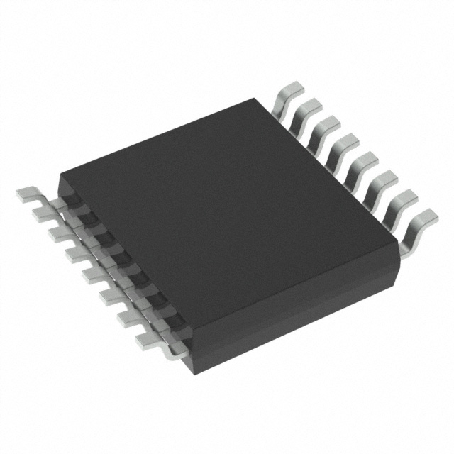
SN74AXC4T245QPWRQ1数据手册规格书PDF详情
1 Features
• AEC-Q100 qualified for automotive applications
• Available in wettable flank QFN (WBQB) package
• Fully-configurable dual-rail design allows each port
to operate with a power supply range from 0.65 V
to 3.6 V
• Operating temperature from –40°C to +125°C
• Multiple direction control pins to allow
simultaneous up and down translation
• Glitch-free power supply sequencing
• Up to 380 Mbps support when translating from 1.8
V to 3.3 V
• VCC isolation feature:
– If either VCC input is below 100 mV, all
I/O outputs are disabled and become high
impedance
• Ioff supports partial-power-down mode operation
• Compatible with AVC-family level shifters
• Latch-up performance exceeds 100 mA per JESD
78, class II
• ESD protection exceeds JEDEC JS-001
– 8000-V human-body model
– 1000-V charged-device model
2 Applications
• Infotainment head unit
• ADAS fusion
• ADAS front camera
• Hybrid electric vehicles and electric vehicles
battery management system
• Telematics control unit
3 Description
The SN74AXC4T245-Q1 AEC-Q100 qualified device
is a four-bit non-inverting bus transceiver that uses
two individually configurable power-supply rails. The
device is operational with both VCCA and VCCB
supplies as low as 0.65 V. The A port is designed
to track VCCA, which accepts any supply voltage from
0.65 V to 3.6 V. The B port is designed to track
VCCB, which also accepts any supply voltage from
0.65 V to 3.6 V. Additionally the SN74AXC4T245-Q1
is compatible with a single-supply system.
The SN74AXC4T245-Q1 device is designed for
asynchronous communication between data buses.
The device transmits data from the A bus to the B bus
or from the B bus to the A bus, depending on the logic
level of the direction-control inputs (1DIR and 2DIR).
The output-enable inputs (1 OE and 2 OE) are used
to disable the outputs so the buses are effectively
isolated. The SN74AXC4T245-Q1 device is designed
so the control pins (xDIR and x OE) are referenced to
VCCA.
To ensure the high-impedance state of the level shifter
I/Os during power up or power down, the x OE pins
should be tied to VCCA through a pull-up resistor.
This device is fully specified for partial-power-down
applications using the Ioff current. The Ioff protection
circuitry ensures that no excessive current is drawn
from or to an input, output, or combined I/O that
is biased to a specific voltage while the device is
powered down.
The VCC isolation feature ensures that if either VCCA
or VCCB is less than 100 mV, both I/O ports enter a
high-impedance state by disabling their outputs.
Glitch-Free power supply sequencing allows either
supply rail to be powered on or off in any order while
providing robust power sequencing performance.
| 供应商 | 型号 | 品牌 | 批号 | 封装 | 库存 | 备注 | 价格 |
|---|---|---|---|---|---|---|---|
TI(德州仪器) |
24+ |
N/A |
10928 |
原厂可订货,技术支持,直接渠道。可签保供合同 |
|||
TI(德州仪器) |
24+ |
TSSOP-16 |
57048 |
原厂可订货,技术支持,直接渠道。可签保供合同 |
|||
TI |
24+ |
TSSOP-16 |
10000 |
||||
TI |
2025 |
N/A |
3880 |
全新原装 |
|||
TI |
24+ |
N/A |
16500 |
只做原装正品现货 假一赔十 |
|||
TI |
24+ |
TSSOP16 |
10000 |
只有原装 |
|||
TI |
24+ |
TSSOP16 |
25836 |
新到现货,只做全新原装正品 |
|||
TI(德州仪器) |
25+ |
TSSOP-16 |
500000 |
源自原厂成本,高价回收工厂呆滞 |
|||
TI/ |
23+ |
TSSOP16 |
20000 |
||||
TI/ |
24+ |
TSSOP16 |
5000 |
十年沉淀唯有原装 |
SN74AXC4T245QPWRQ1 资料下载更多...
SN74AXC4T245QPWRQ1 芯片相关型号
- SN74AHCT245N
- SN74AHCT245NSR
- SN74AHCT245PW
- SN74AHCT245PWG4
- SN74AHCT245PWR
- SN74AHCT245PWRE4
- SN74AHCT245PWRG3
- SN74AHCT245PWRG4
- SN74AHCT245RGYR
- SN74AHCT245RKSR
- SN74AXC4T245
- SN74AXC4T245BQB-Q1
- SN74AXC4T245PW-Q1
- SN74AXC4T245-Q1
- SN74AXC4T245-Q1_V05
- SN74AXC4T245RSV-Q1
- SN74HCS164PW
- SN74HCS165BQB
- SN74HCS244DGSR
- SN74HCS244-Q1
- SN74HCS244RKSR
- SN74HCS273
- SN74HCS273-Q1
- SN74LS32M
- SN74LS32MEL
- SN74LV164ADGVR
- SN74LV164ADR
Datasheet数据表PDF页码索引
- P1
- P2
- P3
- P4
- P5
- P6
- P7
- P8
- P9
- P10
- P11
- P12
- P13
- P14
- P15
- P16
- P17
- P18
- P19
- P20
- P21
- P22
- P23
- P24
- P25
- P26
- P27
- P28
- P29
- P30
- P31
- P32
- P33
- P34
- P35
- P36
- P37
- P38
- P39
- P40
- P41
- P42
- P43
- P44
- P45
- P46
- P47
- P48
- P49
- P50
- P51
- P52
- P53
- P54
- P55
- P56
- P57
- P58
- P59
- P60
- P61
- P62
- P63
- P64
- P65
- P66
- P67
- P68
- P69
- P70
- P71
- P72
- P73
- P74
- P75
- P76
- P77
- P78
- P79
- P80
- P81
- P82
- P83
- P84
- P85
- P86
- P87
- P88
- P89
- P90
- P91
- P92
- P93
- P94
- P95
- P96
- P97
- P98
- P99
- P100
- P101
- P102
- P103
- P104
- P105
- P106