位置:CY7C25652KV18-550BZXC > CY7C25652KV18-550BZXC详情
CY7C25652KV18-550BZXC中文资料
CY7C25652KV18-550BZXC数据手册规格书PDF详情
Functional Description
The CY7C25632KV18 and CY7C25652KV18 are 1.8 V Synchronous Pipelined SRAMs, equipped with QDR II+ architecture. Similar to QDR II architecture, QDR II+ architecture consists of two separate ports: the read port and the write port to access the memory array. The read port has dedicated data outputs to support read operations and the write port has dedicated data inputs to support write operations. QDR II+ architecture has separate data inputs and data outputs to completely eliminate the need to “turn-around” the data bus that exists with common I/O devices. Each port is accessed through a common address bus. Addresses for read and write addresses are latched on alternate rising edges of the input (K) clock.
Features
■ Separate independent read and write data ports
❐ Supports concurrent transactions
■ 550 MHz clock for high bandwidth
■ Four-word burst for reducing address bus frequency
■ Double data rate (DDR) interfaces on both read and write ports (data transferred at 1100 MHz) at 550 MHz
■ Available in 2.5 clock cycle latency
■ Two input clocks (K and K) for precise DDR timing
❐ SRAM uses rising edges only
■ Echo clocks (CQ and CQ) simplify data capture in high-speed systems
■ Data valid pin (QVLD) to indicate valid data on the output
■ On-die termination (ODT) feature
❐ Supported for D[x:0], BWS[x:0], and K/K inputs
■ Single multiplexed address input bus latches address inputs for read and write ports
■ Separate port selects for depth expansion
■ Synchronous internally self-timed writes
■ QDR® II+ operates with 2.5 cycle read latency when DOFF is asserted HIGH
■ Operates similar to QDR I device with 1 cycle read latency when DOFF is asserted LOW
■ Available in × 18, and × 36 configurations
■ Full data coherency, providing most current data
■ Core VDD = 1.8 V ± 0.1 V; I/O VDDQ = 1.4 V to VDD [1]
❐ Supports both 1.5 V and 1.8 V I/O supply
■ HSTL inputs and variable drive HSTL output buffers
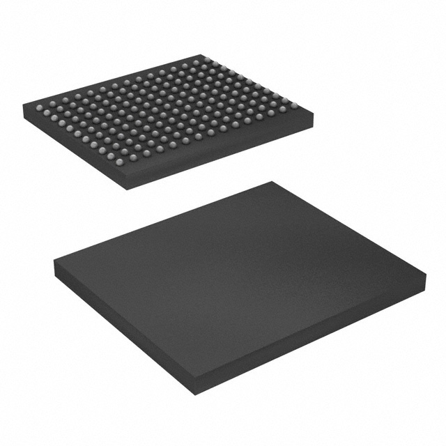
■ Available in 165-ball FBGA package (13 × 15 × 1.4 mm)
■ Offered in both Pb-free and non Pb-free packages
■ JTAG 1149.1 compatible test access port
■ Phase-locked loop (PLL) for accurate data placement
CY7C25652KV18-550BZXC产品属性
- 类型
描述
- 型号
CY7C25652KV18-550BZXC
- 功能描述
静态随机存取存储器 72MB(2Mx36) 1.8v 550MHz DDR II 静态随机存取存储器
- RoHS
否
- 制造商
Cypress Semiconductor
- 存储容量
16 Mbit
- 组织
1 M x 16
- 访问时间
55 ns
- 电源电压-最大
3.6 V
- 电源电压-最小
2.2 V
- 最大工作电流
22 uA
- 最大工作温度
+ 85 C
- 最小工作温度
- 40 C
- 安装风格
SMD/SMT
- 封装/箱体
TSOP-48
- 封装
Tray
| 供应商 | 型号 | 品牌 | 批号 | 封装 | 库存 | 备注 | 价格 |
|---|---|---|---|---|---|---|---|
CYPRESS/赛普拉斯 |
2025+ |
BGA |
5000 |
原装进口价格优 请找坤融电子! |
|||
Cypress |
165-FBGA |
6200 |
Cypress一级分销,原装原盒原包装! |
||||
CYPRESS |
25+ |
BGA-165 |
36 |
就找我吧!--邀您体验愉快问购元件! |
|||
Cypress |
25+ |
25000 |
原厂原包 深圳现货 主打品牌 假一赔百 可开票! |
||||
CYPRESS |
23+ |
BGA-165 |
8560 |
受权代理!全新原装现货特价热卖! |
|||
Cypress |
25+ |
电联咨询 |
7800 |
公司现货,提供拆样技术支持 |
|||
CYPRESS |
22+ |
5000 |
只做原装鄙视假货15118075546 |
||||
Cypress(赛普拉斯) |
25+ |
封装 |
500000 |
源自原厂成本,高价回收工厂呆滞 |
|||
Cypress Semiconductor Corp |
25+ |
165-LBGA |
9350 |
独立分销商 公司只做原装 诚心经营 免费试样正品保证 |
|||
CYPRESS(赛普拉斯) |
24+ |
LBGA165 |
7350 |
现货供应,当天可交货!免费送样,原厂技术支持!!! |
CY7C25652KV18-550BZXC 价格
参考价格:¥2039.8052
CY7C25652KV18-550BZXC 资料下载更多...
CY7C25652KV18-550BZXC 芯片相关型号
- 01108.41.01
- 01358.41T.01
- 01444
- 07611236
- 284TBAS103B26BT
- 284TBCR102B26BT
- 284TCDF102B26BT
- CGJ2C2X7R0J102JTXXXX
- CGJ2F2X7R1H010JTXXXX
- CGJ3H2C0G0J102JTXXXX
- CGJ4H2X7R1H010JTXXXX
- CGJ4L2C0G1H010JTXXXX
- CGJ5B2X7R0J102JTXXXX
- CGJ5C2X7R1C101J
- CKD31BJB1E225S(085A)
- CY7C1327G_12
- CY7C1360C-166AXC
- CY7C25632KV18-500BZXC
- EMS22D31-M28-WS4
- EMS22D31-R25-WS4
- EMS22D53-C16-WS4
- EMS22Q53-M25-WS3
- ICL3217E
- ISL3152E
- NVD6824NL
- Y-CONC-R426PFE6P-2000-C
- Y-CONC-R602LRJ6P-2000-C
- Y-CONC-R62CU-MB8A-2000-A
- Y-CONC-R802MCU6P-2000-C
- Y-CONC-R80CURJ6P-2000-C
CYPRESS相关芯片制造商
Datasheet数据表PDF页码索引
- P1
- P2
- P3
- P4
- P5
- P6
- P7
- P8
- P9
- P10
- P11
- P12
- P13
- P14
- P15
- P16
- P17
- P18
- P19
- P20
- P21
- P22
- P23
- P24
- P25
- P26
- P27
- P28
- P29
- P30
- P31
- P32
- P33
- P34
- P35
- P36
- P37
- P38
- P39
- P40
- P41
- P42
- P43
- P44
- P45
- P46
- P47
- P48
- P49
- P50
- P51
- P52
- P53
- P54
- P55
- P56
- P57
- P58
- P59
- P60
- P61
- P62
- P63
- P64
- P65
- P66
- P67
- P68
- P69
- P70
- P71
- P72
- P73
- P74
- P75
- P76
- P77
- P78
- P79
- P80
- P81
- P82
- P83
- P84
- P85
- P86
- P87
- P88
- P89
- P90
- P91
- P92
- P93
- P94
- P95
- P96
- P97
- P98
- P99
- P100
- P101
- P102
- P103
- P104
- P105
- P106
- P107