位置:S29JL064J55TFI000 > S29JL064J55TFI000详情
S29JL064J55TFI000中文资料
S29JL064J55TFI000数据手册规格书PDF详情
Software Features
Supports Common Flash Memory Interface (CFI)
Erase suspend/erase resume
– Suspends erase operations to read data from, or program data to, a sector that is not being erased, then resumes the erase operation
Data# polling and toggle bits
– Provides a software method of detecting the status of program or erase operations
Unlock bypass program command
– Reduces overall programming time when issuing multiple program command sequences
Hardware Features
Ready/Busy# output (RY/BY#)
– Hardware method for detecting program or erase cycle completion
Hardware reset pin (RESET#)
– Hardware method of resetting the internal state machine to the read mode
WP#/ACC input pin
– Write protect (WP#) function protects sectors 0, 1, 140, and 141, regardless of sector protect status
– Acceleration (ACC) function accelerates program timing
Sector Protection
– Hardware method to prevent any program or erase operation within a sector
– Temporary Sector Unprotect allows changing data in protected sectors in-system
General Description
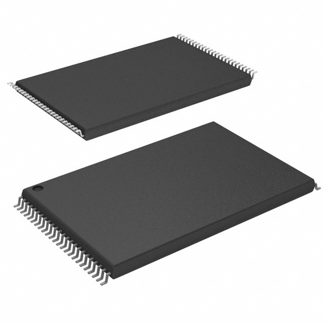
The S29JL064J is a 64 Mbit, 3.0 volt-only flash memory device, organized as 4,194,304 words of 16 bits each or 8,388,608 bytes of 8 bits each. Word mode data appears on DQ15–DQ0; byte mode data appears on DQ7–DQ0. The device is designed to be programmed in-system with the standard 3.0 volt VCC supply, and can also be programmed in standard EPROM programmers. The device is available with an access time of 55, 60, 70 ns and is offered in a 48-ball FBGA or 48-pin TSOP package. Standard control pins—chip enable (CE#), write enable (WE#), and output enable (OE#)—control normal read and write operations, and avoid bus contention issues. The device requires only a single 3.0 volt power supply for both read and write functions. Internally generated and regulated voltages are provided for the program and erase operations.
S29JL064J55TFI000产品属性
- 类型
描述
- 型号
S29JL064J55TFI000
- 功能描述
闪存 64Mb 3V 55ns Parallel NOR 闪存
- RoHS
否
- 制造商
ON Semiconductor
- 数据总线宽度
1 bit
- 存储类型
Flash
- 存储容量
2 MB
- 结构
256 K x 8
- 接口类型
SPI
- 电源电压-最大
3.6 V
- 电源电压-最小
2.3 V
- 最大工作电流
15 mA
- 工作温度
- 40 C to + 85 C
- 安装风格
SMD/SMT
- 封装
Reel
| 供应商 | 型号 | 品牌 | 批号 | 封装 | 库存 | 备注 | 价格 |
|---|---|---|---|---|---|---|---|
CYPRESS/赛普拉 |
TSOP-48 |
1143 |
公司现货库存,代理分出来的货 |
||||
CYPRESS |
24+ |
TSOP |
2444 |
原厂直供,支持账期,免费供样,技术支持 |
|||
CYPRESS |
24+ |
TSOP-48 |
12000 |
进口原装 价格优势 |
|||
CYPRESS/赛普拉斯 |
25+ |
TSOP48 |
13800 |
原装,请咨询 |
|||
Cypress / Spansion |
23+ |
NA |
8800 |
只做原装正品现货 |
|||
CYPRESS/赛普拉斯 |
23+ |
TSOP48 |
98900 |
原厂原装正品现货!! |
|||
Cypress(赛普拉斯) |
24+ |
TSOP-48 |
42432 |
原厂可订货,技术支持,直接渠道。可签保供合同 |
|||
Cypress |
22+ |
48TSOP (18.4x12) |
9000 |
原厂渠道,现货配单 |
|||
Cypress |
13+ |
TSOP-48 |
345 |
一级代理,专注军工、汽车、医疗、工业、新能源、电力 |
|||
CYPRESS |
24+ |
TSOP-48 |
3139 |
假一赔百原装正品价格优势实单可谈 |
S29JL064J55TFI000 价格
参考价格:¥22.4795
S29JL064J55TFI000 资料下载更多...
S29JL064J55TFI000 芯片相关型号
- 13703
- 13704
- ADAQ4224
- BZG03C180
- DCH010512D
- DCH010512DN7
- DCH010512DN7.B
- DCH010512S
- DCH010512SN7
- DCH010512SN7.B
- DCH010515D
- ELJRF15NDFB
- ELJRF15NJFB
- LM2841XMKX-ADJLSLASHNO.A
- LM2841XMKX-ADJLSLASHNOPB
- LM2841XQMKSLASHNOPB
- LM2841XQMKSLASHNOPB.A
- LM8330
- LM8330TMESLASHNOPB
- LM8330TMESLASHNOPB.A
- LM8330TMXSLASHNOPB
- P4SMA200CA
- S29GL01GS11DAIV10
- S29JL064J55BFI000
- S29JL064J55BFI003
- S29JL064J55BHI000
- S29JL064J55BHI003
- S29JL064J55TFI003
- S29JL064J55THI000
- S29JL064J55THI003
CYPRESS相关芯片制造商
Datasheet数据表PDF页码索引
- P1
- P2
- P3
- P4
- P5
- P6
- P7
- P8
- P9
- P10
- P11
- P12
- P13
- P14
- P15
- P16
- P17
- P18
- P19
- P20
- P21
- P22
- P23
- P24
- P25
- P26
- P27
- P28
- P29
- P30
- P31
- P32
- P33
- P34
- P35
- P36
- P37
- P38
- P39
- P40
- P41
- P42
- P43
- P44
- P45
- P46
- P47
- P48
- P49
- P50
- P51
- P52
- P53
- P54
- P55
- P56
- P57
- P58
- P59
- P60
- P61
- P62
- P63
- P64
- P65
- P66
- P67
- P68
- P69
- P70
- P71
- P72
- P73
- P74
- P75
- P76
- P77
- P78
- P79
- P80
- P81
- P82
- P83
- P84
- P85
- P86
- P87
- P88
- P89
- P90
- P91
- P92
- P93
- P94
- P95
- P96
- P97
- P98
- P99
- P100
- P101
- P102
- P103
- P104
- P105
- P106